Micro-Line
The μ-Line (Micro-Line) is a wafer post-processing and test facility tailored for next generation defense microelectronics applications.

Wafer Post Processing
The μ-Line facility for semiconductor wafer post-processing provides Northrop Grumman with an assured source for the development and production of critical microelectronics packaging technologies. Products processed at the μ-Line will serve as essential building blocks to some of the world’s most advanced radio frequency (RF) and electro-optic infrared (EO/IR) defense systems.

Capabilities
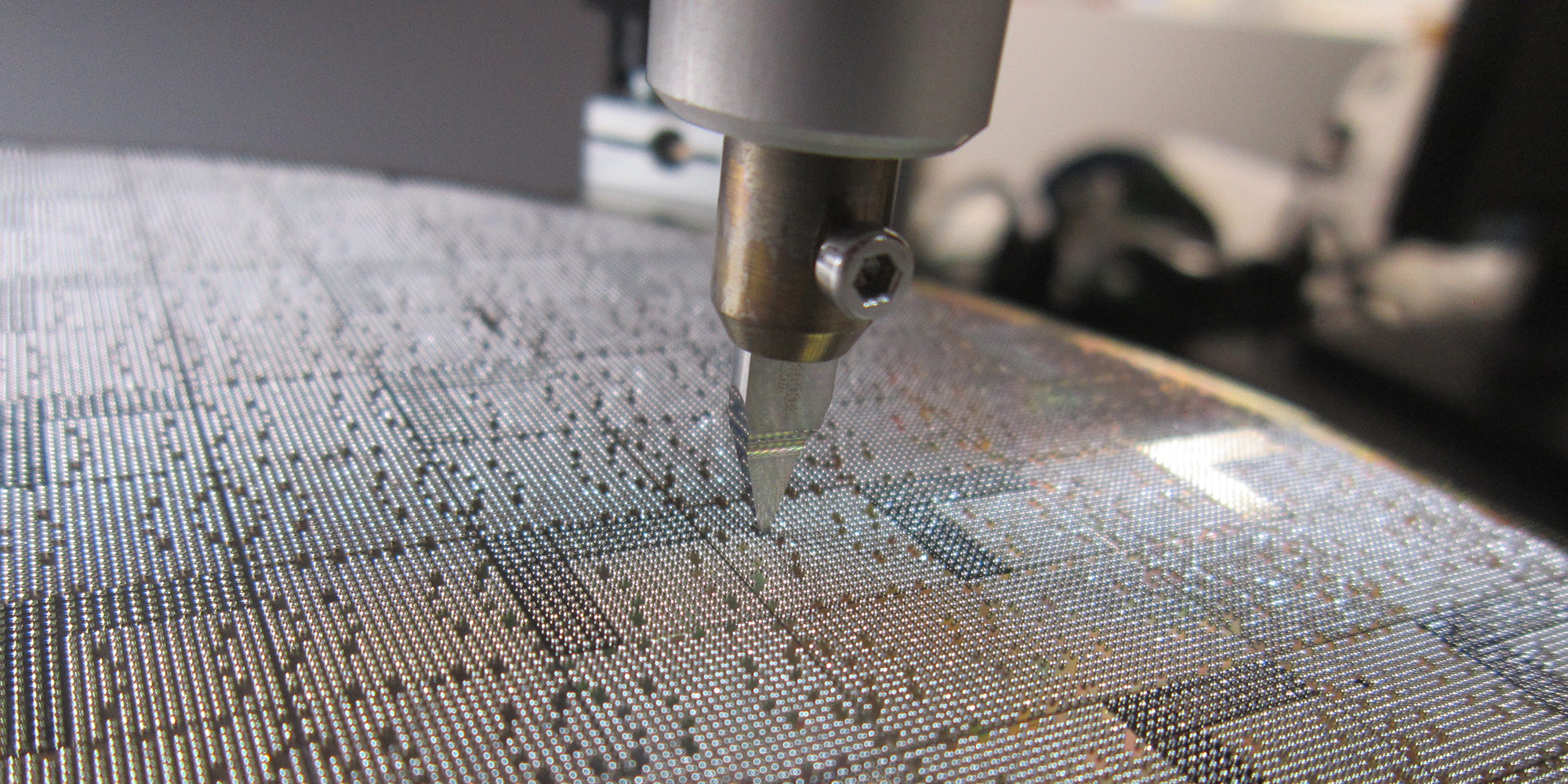
Wafer Bumping
- Dielectric passivation, underbump metallization, and solder bumping processes for 100 mm to 300 mm semiconductor wafers
- Bumping processes include solder ball transfer and solder-capped copper pillars with tin-lead alloys
Dicing
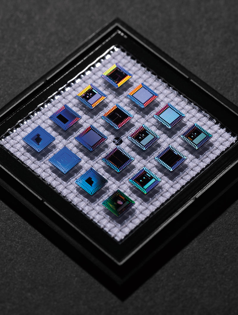
- Mechanical saw dicing, thinning, and polishing
- Die-level laser marking, picking, and sorting

Advanced Inspection & Metrology
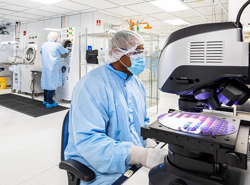
- Full-wafer 2D/3D automated optical inspection for physical defect tracking and yield mapping
- Plating bath and solder alloy chemistry analysis, and wafer-level bump shear for process and material quality control
Wafer Testing
- Electrical probing/testing for unbumped wafers, bumped wafers, or bumped die up to 300 mm diameter
- Test yield tracking integrated with physical yield/defect mapping for overall die yield screening


